‘Fab Future’ for India
August 4, 2021 | Expert Insights
Dr. C.S. Rao Dr. C.S. Rao is the Chairman and Co-Founder of QuadGen Wireless Solutions Inc. He is also the President of the Association of Unified Telecom Service Providers of India (AUSPI).
India’s ambitious social objectives of universal education, health care, agriculture growth, booming commerce, and reliable and efficient banking, are all dependent on the ‘3-Cs’- Connectivity, Command and Control and Cloud Computing applications. To achieve this level of digitisation, which is unprecedented, the country will need to muster the power of silicon.
Currently, the era of digital transformation is being driven through several government initiatives - Digital India, Skill India, Smart City India, Make in India etc. The investment in all these sectors must be aligned to build the ‘Fab of Future’ for India. This is a compelling necessity, if India has to exploit the growth potential of consumer electronics, mobile communication, connected electric grids, connected smart enterprise networks and industrial automation-driven smart manufacturing.
Over the next few years, next-generation technologies will revolutionise the way we do business. Apart from 5G, technologies like Wi-Fi 6, Multi-access Edge Computing (MEC) and Cloud Computing will be rolled out between 2021 and 2025. Moreover, Wi-Fi 7 and 6G are expected to become operational between 2025 to 2030. Connected vehicles, threat intelligence-based cybersecurity etc. are other promising demand drivers for the massive scale of 6 -10 B endpoint devices in India that require Very Large Scale Integrated (VLSI)-based chips.
DEMAND EXCEEDING SUPPLY
The global chip shortage is posing a serious threat to societal welfare, akin to the COVID pandemic witnessed over the last few months. The level of electronic goods imports by India makes a compelling business case for establishing fab facilities in the country. Other countries have already recognised this and have taken the lead. The U.S. has committed $ 50 billion federal investment through the United States Innovation and Competition Act (USICA) for semiconductor manufacturing, research and design initiatives. Along similar lines, China, South Korea, and the EU have earmarked up to $250 billion as government investment over the next decade, for the growth of the semiconductor industry segment.
Furthermore, nineteen new fabs will be operating by the end of 2021, and another ten will join by 2022. The fab industry is looking at an investment of over $140 billion to meet the accelerating demand of chips across the wide range of market segments, including 5G/Cloud/ MEC/Industrial Internet of Things/ Health Care/Connected Vehicles/Security and Surveillance. It is further predicted that the worldwide integrated circuit (IC) market would top $500 billion in 2021.
INDIA’S OPTIONS
Over the last three decades, despite many inter-departmental confabulations, there has been very little progress in establishing a fab industry in India. Therefore, the government must reassess the situation across the entire semiconductor value chain and act to roll out a new ‘Fab of Future’ policy. India cannot afford to lose any more time in the creation of a long-lasting industry base for semiconductor manufacturing in the country.
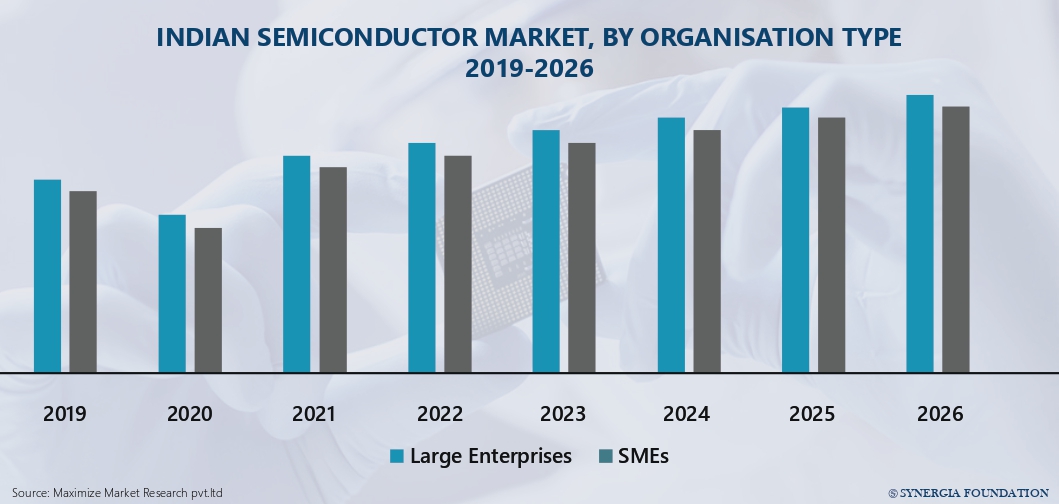
By 2023, India must establish a fab facility of 200 mm wafer production to meet the demand patterns in consumer electronics, mobile communication and the information technology (IT) segments industry with cloud architecture-based data centre growth. Indian silicon domain specialists estimate that there is a need for about 100K wafers per month of 200 mm equivalents.
Establishing a fab over the next two years will surely ensure a kind of economic security for India in digital sectors by 2024. Indian fab facility creation has to start from the 20nm level and should have the capability to handle up to 7nm in the next four years. The investment for such a 200 mm greenfield fab will cost at least US $2 billion and take approximately 18 months to establish and start production. In this regard, India may consider the provision of funding along the lines of the U.S. Chip Act. To incentivise fab manufacturing and research, there is also a need for semiconductor investment tax credit. A model already exists in the ‘Facilitating American Built Semiconductors Act (FABS)’ in the U.S., which is a bipartisan legislation.
India must guard against global semiconductor supply chain vulnerabilities, as geopolitical tensions involving China, Taiwan, Israel and the U.S. could lead to export restrictions of silicon ICs. A homegrown fab would ensure that India has safeguards against a potential unilateral threat in silicon supplies. India has to evolve its own unique model, drawing on hitherto established frameworks in the U.S. and China.
HOMEGROWN TALENT
India has a proven and experienced talent pool in application-specific integrated circuit (ASIC) design, validation, reference circuit design service, electronic design automation (EDA), storage technology such as DRAM and NAND, real-time embedded design as well as physical computer-aided design (CAD) methodology. It also has expertise and exposure in AL-ML based techniques and tools that can drive the automation level required to scale up the digital chip design complexity.
The industry promises a significant spurt in job opportunities with a proven job multiplier factor of 6 - every job in the semiconductor industry enables the creation of five more jobs. The jobs could be in the range of 60K to 80 K for design, verification, validation, testing etc. and an additional 100 K for other related jobs. It is estimated that in the U.S., a federal investment of $50 billion will have a 4x multiplier effect on the U.S. economy over the next five years.
STATE-OF-THE-ART TRENDS
The industrial growth in central processing units(CPU) and graphics processing units(GPU) is currently at 30 per cent year-on-year. Meanwhile, the Super Computing/High-Performance Computing (HPC) is at 50 per cent year-on-year, which will further drive the growth in CPU/GPU and NAND storage. Moreover, the internet exchange traffic has reached a world record of 9 TBps at Frankfurt. This trend will further drive data center and CPU growth.
Moore's law will continue for the next 5-7 years at the very least, with respect to CMOS transistor density of packing on substrates. For 7nm nodes, the technology behind Moore's law continuation is Extreme Ultraviolet Lithography (EUV). The next revolution for 1 nm is High Numerical Aperture EUV (HNA_EUV). Front End of Line (FEOL) device architecture is another driver for Moore’s law continuity. In this context, India needs to account for the lightning speed at which computing technology is advancing.


Comments