Moving Beyond Silicon
August 6, 2021 | Expert Insights

Dr. R Muralidharan is an Emeritus Professor at the Indian Institute of Science IISc). This article is based on his views at the 104th virtual forum on ‘Semiconductors and Supply Chains in Asia’, jointly organised by the Synergia Foundation and the Taiwan Center for Security Studies.
There is a huge gap between India and the world in electronics manufacturing. Bridging this gap is a strategic and economic necessity. In fact, there are ongoing efforts by the Government of India to establish a complementary metal-oxide semiconductor (CMOS) foundry in the country.
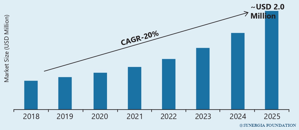
Generally, the fab is perceived as a silicon foundry of sub-50 nm or sub-100 nm gate length and feature size. However, there are other emerging areas like Gallium Nitride (GaN) electronics that also show potential. Like silicon, they can be extremely useful in supporting sub-systems like e-vehicles, power converters, solar inverters etc. GaN RF electronics have also emerged as a key technology for 5G applications.
Establishing fabs for the production of GaN devices is relatively less expensive. The obsolescence rate is also not high. All these factors make a strong case for setting up a foundry that focuses on both materials and device production. The Indian Institute of Science (IISc) has submitted a detailed project report on establishing a GaN foundry to the Government of India.
The semiconductor industry, however, is a long-term investment that is capital intensive. In most countries, governments have either completely funded the initial nucleation or infused funds into foundries, as and when needed, to maintain a strategic edge.
It is well-established that the backbone of semiconductor production is situated in Taiwan. They have also established a strong base in the field of GaN technology. Against this backdrop, compound semiconductors form a possible avenue for bilateral collaboration between India and Taiwan. It could form a base for Taiwanese chip companies to diversify their investments in India, eventually creating a supply chain centre of excellence.
To support this endeavour, India has a wealth of human resources. Academic institutions like the IISc, the Indian Institutes of Technology (IITs) as well as national laboratories have sufficient expertise to address technical challenges relating to GaN fabs. As part of various government initiatives over the past fifteen years, students have also been trained in ‘fab-like’ facilities, where they learn the techniques and designs employed in semiconductor manufacturing.
Currently, however, such skilled manpower is forced to pursue employment opportunities abroad. By facilitating the right ecosystem in India, their talent can be effectively utilised in the country.


Comments